#
The HSI Clock is the clock signal generated by its internal RC oscillator. In STM32F108C6 it is of 8 MHz and by default after power-on/System Reset it is used as main system clock (SYSCLK).
I cannot resist my self to bring my analogy for MCU Clock source and clock signal is that this MCU is operating on internal heart (RC oscillator) which is beating at the rate of 8 MHz. Which simply means this heart is beating every (1/(8 * 10^6)) Seconds = 125 ns (Clock Period). And it will beat (10^9)/125 = 8000000 times per sec (Numbers of Clock Period in one seconds).
But is there any way through which i can see this clock signal (Heart beats) and also measures its frequency (Heart Rate).
Okay Let me formulate it as an Task.
So now the task is to output this clock to MCU I/O pin and measure its frequency with the help of some tool.
The approach to this task is as follows:
-
Output the Clock on Microcontroller Output pin (MCO) (Basically via writing Code)
-
Select the desired clock for the MCO signal.
-
Output the MCO Signal to MCU MCO pin.
-
-
Capturing the signal on MCO pin using Logic Analyzer/Oscilloscope.
Lets Accomplish this Task
1) First lets find out MCOx pin on STM32F103C8 using its Datasheet
Please find Datasheet here /Datasheet/stm32f103c8.pdf
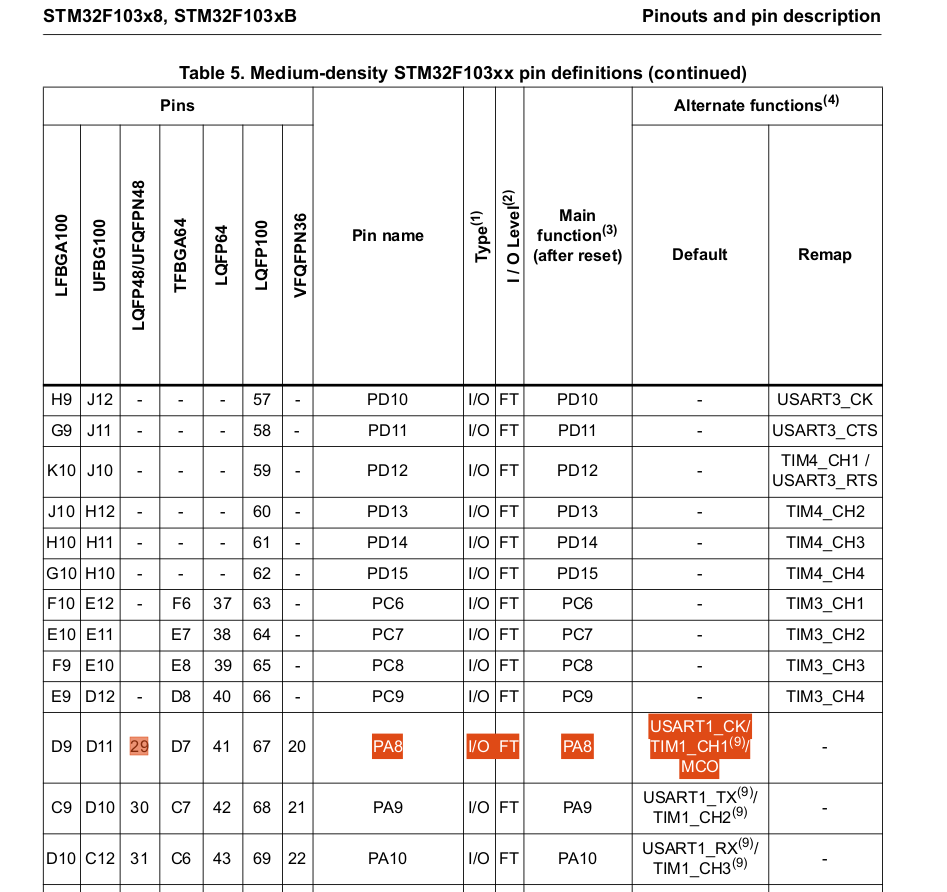
From the above image PA8 pin can be configured as MCO pin.
2) Now lets explore the register for making PA8 as MCO pin using STM32F108C8 Reference Manaual
Please find Datasheet here /Datasheet/STM32F103xx_Ref_Manual.pdf
A) Configuring MCO bit fields in RCC_CFGR register to select HSI as Clock Source
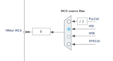
We have multiple option to select Clock Source (PLL, HSE, HSI), but currently I am interested in HSI.
Lets Look at RCC_CFGR Register.

To select HSI Clock we need to write 101 (5 in Decimal) in MCO[3:0] (Bit 26 to Bit 24 of RCC_CFGR). So lets write code for it.
    #define  RCC_BASE_ADDR     0x40021000U    // Base address of RCC Registers

    #define  RCC_CFGR_OFFSET   0x00000004U    // Offset address of RCC_CFGR

    #define   RCC_CFGR_ADDR   0x40021004U  //RCC_BASE_ADDR + RCC_CFGR_OFFSET

    uint32_t *pRccCfgrReg =  (uint32_t*) RCC_CFGR_REG_ADDR; //Derefrencing RCC_CFGR Address

    *pRccCfgrReg &= ~(0x7 << 24);     // Clear Bits 26 to 24

    *pRccCfgrReg |= (0x5 << 24);       // 0101 << 24
B) Configuring PA8 as MCO pin


At first enable the clock for peripheral GPIOA port.


So lets write code for enabling GPIOA Clock. Please remember if peripheral clock is disabled, that peripheral will not respond to any configuration.
    #define RCC_APB2ENR_OFFSET  0x00000018U // Offset address of RCC_APB2ENR Register

    #define RCC_APB2ENR_ADDR  (RCC_BASE_ADDR + RCC_APB2ENR_OFFSET)

    //a ) Enable the peripheral clock for GPIOA peripheral

	 uint32_t *pRccApb2enrReg = (uint32_t*)RCC_APB2ENR_ADDR;

	*pRccApb2enrReg |= ( 1 << 2); //Enable GPIOA peripheral clock
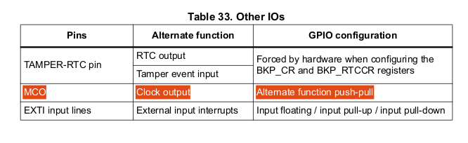
Now to make PA8 as MCO pin do the following configuration in GPIO_CRH register.
Mode: Output mode, max speed 50 MHz.
Configuration: Alternate function output Push-pull and Speed at 50 MHz.
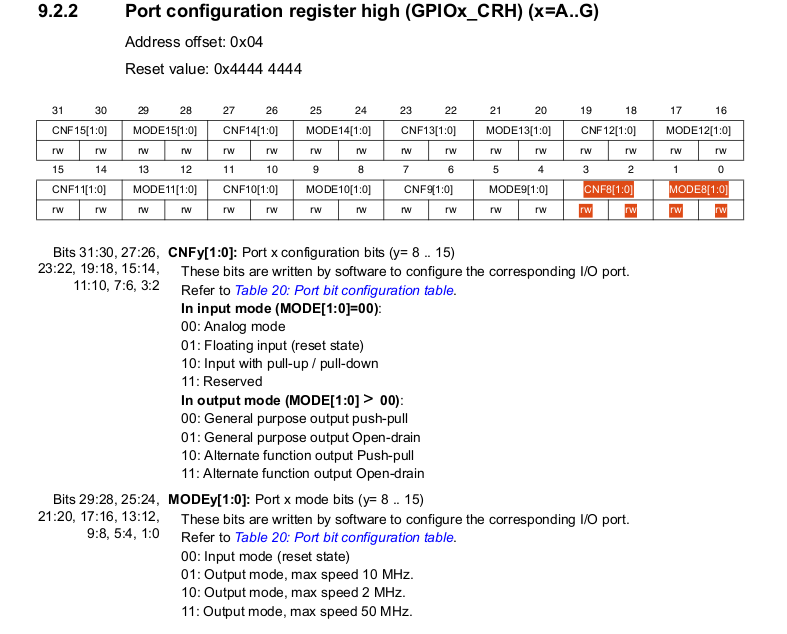
Lets write a code for Configuring PA8 pin as MCO pin (Alternate Function).
    #define GPIOA_BASE_ADDR 0x40010800U // Base address of GPIOA

    #define GPIOA_CRH_OFFSET  0X00000004U //Offset address of GPIO_CRH

    #define GPIOA_CRH_ADDR   (GPIOA_BASE_ADDR + GPIOA_CRH_OFFSET) //Address of GPIOA_CRH

    /b ) Configure the mode of GPIOA pin 8 as alternate function mode

    uint32_t *pGpioACrhReg = (uint32_t*)GPIOA_CRH_ADDR; // Dereference the GPIOA_CRH address

    *pGpioACrhReg &= ~(0xF << 0); // clear bit 0 to 3

    *pGpioACrhReg |= 0x9; // write 1001 to Bits[3:0] of GPIOA_CRH
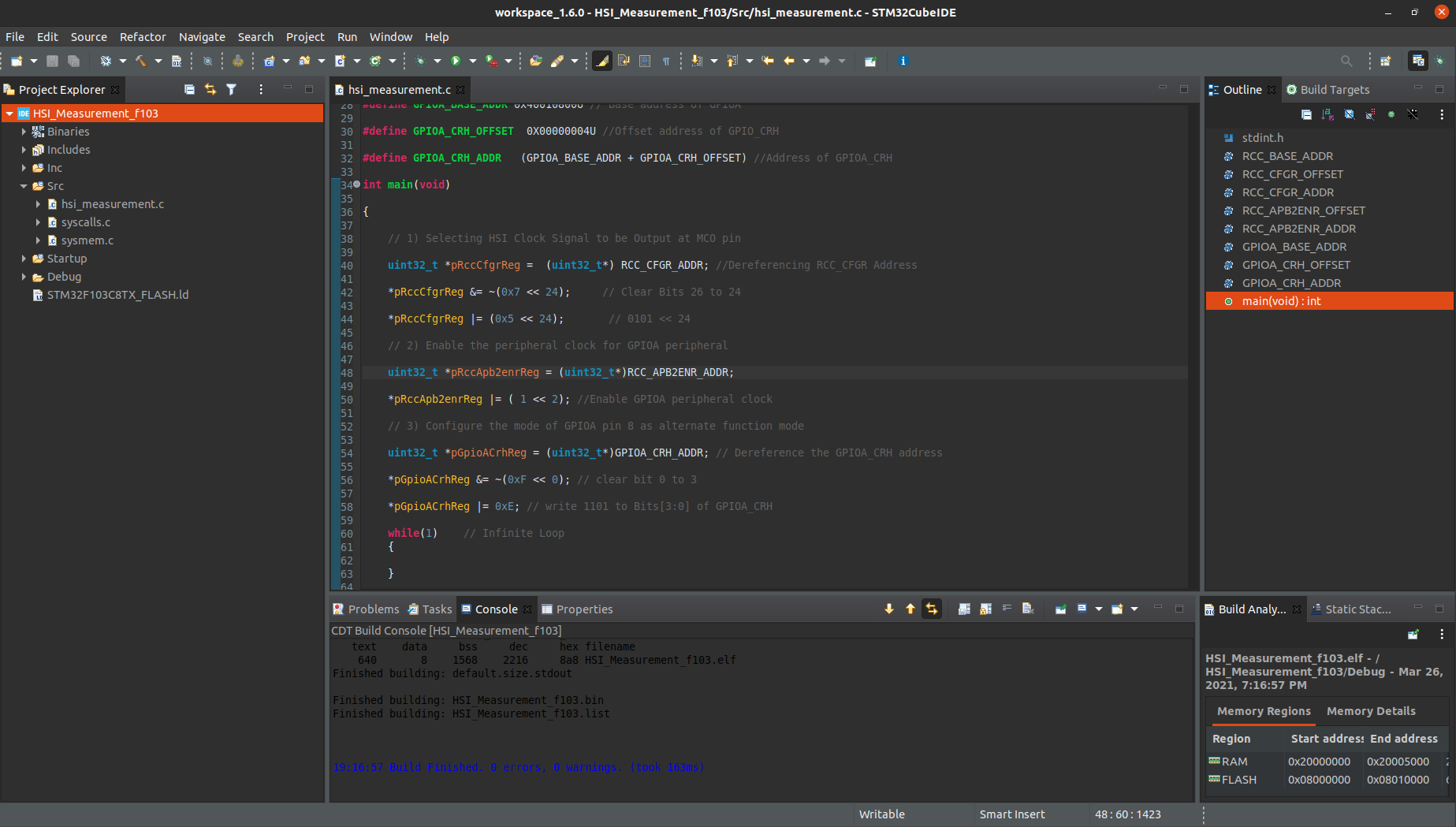
Cool, so we are almost done to this task. Lets summarize what we have done so far and then will organize the above multiple pieces of code into a single functioning code.
Configure the RCC_CFGR MCO bit to select HSI as clock source.
Enable the peripheral clock for GPIOA peripheral.
Configure the mode of GPIOA pin 8 as alternate function mode.
    /**
    ******************************************************************************
    * @file    HSI_CLK_OMM.c
    * @author  Ashish Kumar Pardeshi
    * @brief   This code will Ouput the HSI clock at MCO pin (PA8).
    ******************************************************************************
    */
    #include<stdint.h>

    // Making RCC_CHGR Register Address

    #define  RCC_BASE_ADDR     0x40021000U    // Base address of RCC Registers

    #define  RCC_CFGR_OFFSET   0x00000004U    // Offset address of RCC_CFGR

    #define   RCC_CFGR_ADDR   0x40021004U  //RCC_BASE_ADDR + RCC_CFGR_OFFSET

    // Making RCC_APB2ENR Register Address

    #define RCC_APB2ENR_OFFSET  0x00000018U // Offset address of RCC_APB2ENR Register

    #define RCC_APB2ENR_ADDR  (RCC_BASE_ADDR + RCC_APB2ENR_OFFSET)

    // Making GPIOA_CRH Register Address

    #define GPIOA_BASE_ADDR 0x40010800U // Base address of GPIOA

    #define GPIOA_CRH_OFFSET  0X00000004U //Offset address of GPIO_CRH

    #define GPIOA_CRH_ADDR   (GPIOA_BASE_ADDR + GPIOA_CRH_OFFSET) //Address of GPIOA_CRH

    int main(void)

    {

      // 1) Selecting HSI Clock Signal to be Output at MCO pin

      uint32_t *pRccCfgrReg =  (uint32_t*) RCC_CFGR_ADDR; //Derefrencing RCC_CFGR Address

      *pRccCfgrReg &= ~(0x7 << 24);     // Clear Bits 26 to 24

      *pRccCfgrReg |= (0x5 << 24);       // 0101 << 24

      // 2) Enable the peripheral clock for GPIOA peripheral

      uint32_t *pRccApb2enrReg = (uint32_t*)RCC_APB2ENR_ADDR;

      *pRccApb2enrReg |= ( 1 << 2); //Enable GPIOA peripheral clock

      // 3) Configure the mode of GPIOA pin 8 as alternate function mode

      uint32_t *pGpioACrhReg = (uint32_t*)GPIOA_CRH_ADDR; // Dereference the GPIOA_CRH address

      *pGpioACrhReg &= ~(0xF << 0); // clear bit 0 to 3

      *pGpioACrhReg |= 0xB; // write 1011 to Bits[3:0] of GPIOA_CRH

      while(1)    // Infinite Loop
      {

      }

    }
This code and complete STMCubeIDE workspace can also be found at /HSI_Measurement_f103
Okay time to compile and upload this code to target (STM32F103C8 (Bluepill Board)) then connecting MCO pin to logic analyzer to view the HSI clock signal.
I have succesfully uploaded the Hex file using STLink_V2 Programmer/Debugger and also captured the HSI Clock Signal at PA8 (MCO) pin using 24 MHZ Logic Analyzer.
Here is the screenshot.
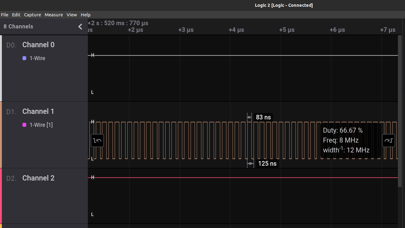
The Clock signal is visible with following specifications:
Frequency: 8 MHz
Clock Cycle Period: 125 ns
Duty Cycle: 66.67 %
Width: 12 MHz
So here the frequency and Clock Cycle period is measured correctly but Duty cycle should be 50 % instead of 66.67%.